
为 ThinkPad X230 刷 Coreboot (
预备知识
- coreboot,原名LinuxBIOS,是一个旨在取代大多数计算机中专有韧体(BIOS或UEFI)的软件项目, 它采用轻量级固件设计,只执行加载和运行现代32位或64位操作系统所需的最少量任务。
- me_cleaner 是一个移除固件中 Intel Management Engine 中非关键部分的 Python 脚本, 可以和 coreboot 结合使用。
- Intel Management Engine 是一個擁有從底層控制硬件能力的、獨立與處理器和操作系統的框架, 它對於操作系統也是隱形的。簡單點說就是擁有極高的權限。 其中 Intel Active Management Technology(英特爾主動管理技術) 是運行與 ME 框架上的應用的一個例子。 (因为权限大又没有审计又经常爆出漏洞偶尔被戏称为 Malicious Engine)
关于 Intel Malicious Management Engine 的问题
某只咸鱼 写的还算清楚,推荐去读一读。
其实就是想去掉原厂 BIOS 里的白名单而已……
开始前要准备些啥?
- 一台 X230 (这不是废话嘛)
- 知道这样做可能会把电脑搞砖的风险(
- 一个编程器
- 另一台电脑(用于编译 coreboot 和操作编程器)
- 热风和焊接工具(用于取下 BIOS IC)
- 或者 SOP-8 测试夹(如果对自己的焊接技术没信心的话,
比如咱……)
取得 coreboot 和 flashrom 的源代码和制作工具链
日常 git 两连:
git clone https://review.coreboot.org/coreboot.git
git clone https://review.coreboot.org/flashrom.git
安装制作工具链需要的依赖(如果是 Arch 的话,其他的系统就只好自己发挥了 😂)
pacman -S base-devel gcc-ada nasm
从 AUR 装 uefitool-git(后面提取 VGA BIOS 需要)
然后在 coreboot 的目录下制作工具链:
make crossgcc
其它的选项和用法去看看 make help 咯 😂
备份原有固件和取出其中的 Blob
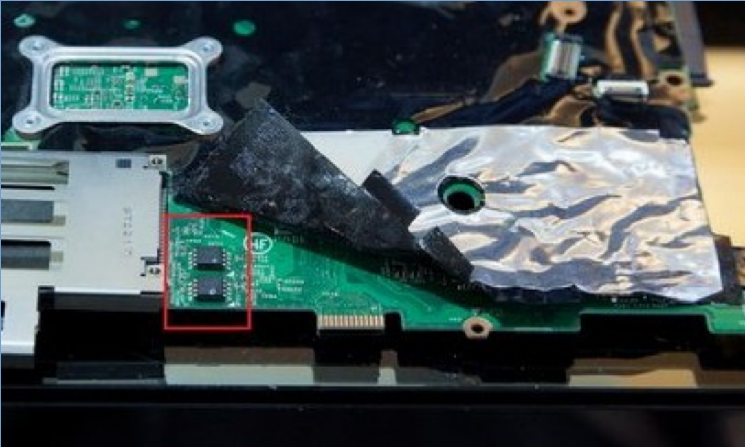
拆开电脑的掌托,揭开防静电贴纸就能看到两块 BIOS 芯片啦……
然后拿出编程器在另一台电脑上开始 Dump 固件吧,例如这样:
flashrom 命令依编程器而异,不要照抄 😂
flashrom -p linux_spi:dev=/dev/spidev0.0 -r top.rom -c MX25L3206E/MX25L3208E
flashrom -p linux_spi:dev=/dev/spidev0.0 -r bottom.rom -c MX25L6406E/
然后接起来:
cat bottom.rom top.rom > complete.rom
最好多做几次然后验证一下散列值(为了确保备份的固件不是坏的?)
使固件可写(ifdtool 在 coreboot/utils 里)
$ ~/repo/coreboot/util/ifdtool/ifdtool -u complete.rom
File complete.rom is 12582912 bytes
Writing new image to complete.rom.new
用 me_cleaner 清除非必需 ME 固件(也在 coreboot/utils 里)
$ ~/repo/coreboot/util/me_cleaner/me_cleaner.py complete.rom.new
Full image detected
The ME/TXE region goes from 0x3000 to 0x500000
Found FPT header at 0x3010
Found 23 partition(s)
Found FTPR header: FTPR partition spans from 0x183000 to 0x24d000
ME/TXE firmware version 8.1.30.1350
Removing extra partitions...
Removing extra partition entries in FPT...
Removing EFFS presence flag...
Correcting checksum (0x7b)...
Reading FTPR modules list...
UPDATE           (LZMA   , 0x1cf4f2 - 0x1cf6b0): removed
ROMP             (Huffman, fragmented data    ): NOT removed, essential
BUP              (Huffman, fragmented data    ): NOT removed, essential
KERNEL           (Huffman, fragmented data    ): removed
POLICY           (Huffman, fragmented data    ): removed
HOSTCOMM         (LZMA   , 0x1cf6b0 - 0x1d648b): removed
RSA              (LZMA   , 0x1d648b - 0x1db6e0): removed
CLS              (LZMA   , 0x1db6e0 - 0x1e0e71): removed
TDT              (LZMA   , 0x1e0e71 - 0x1e7556): removed
FTCS             (Huffman, fragmented data    ): removed
ClsPriv          (LZMA   , 0x1e7556 - 0x1e7937): removed
SESSMGR          (LZMA   , 0x1e7937 - 0x1f6240): removed
The ME minimum size should be 1667072 bytes (0x197000 bytes)
The ME region can be reduced up to:
00003000:00199fff me
Checking the FTPR RSA signature... VALID
Done! Good luck!
用 ich_descriptors_tool 取出 blob(这个在 flashrom/util 里):
$ ~/repo/flashrom/util/ich_descriptors_tool/ich_descriptors_tool -f complete.rom.new -d
The flash image has a size of 12582912 [0xc00000] bytes.
Assuming chipset '6 series Cougar Point'.
=== Content Section ===
FLVALSIG 0x0ff0a55a
FLMAP0   0x03040103
FLMAP1   0x12100206
FLMAP2   0x00210120

--- Details ---
NR          (Number of Regions):                     4
FRBA        (Flash Region Base Address):         0x040
NC          (Number of Components):                  2
FCBA        (Flash Component Base Address):      0x030
ISL         (ICH/PCH Strap Length):                 18
FISBA/FPSBA (Flash ICH/PCH Strap Base Address):  0x100
NM          (Number of Masters):                     3
FMBA        (Flash Master Base Address):         0x060
MSL/PSL     (MCH/PROC Strap Length):                 1
FMSBA       (Flash MCH/PROC Strap Base Address): 0x200

=== Component Section ===
FLCOMP   0x4990001c
FLILL    0x00000000

--- Details ---
Component 1 density:            8 MB
Component 2 density:            4 MB
Read Clock Frequency:           20 MHz
Read ID and Status Clock Freq.: 33 MHz
Write and Erase Clock Freq.:    33 MHz
Fast Read is supported.
Fast Read Clock Frequency:      50 MHz
No forbidden opcodes.

=== Region Section ===
FLREG0   0x00000000
FLREG1   0x0bff0500
FLREG2   0x04ff0003
FLREG3   0x00020001

--- Details ---
Region 0 (Descr. ) 0x00000000 - 0x00000fff
Region 1 (BIOS   ) 0x00500000 - 0x00bfffff
Region 2 (ME     ) 0x00003000 - 0x004fffff
Region 3 (GbE    ) 0x00001000 - 0x00002fff

=== Master Section ===
FLMSTR1  0xffff0000
FLMSTR2  0xffff0000
FLMSTR3  0x08080118

--- Details ---
    Descr. BIOS ME GbE Platf.
BIOS    rw    rw  rw  rw   rw
ME      rw    rw  rw  rw   rw
GbE                   rw

=== Upper Map Section ===
FLUMAP1  0x000018df

--- Details ---
VTL (length in DWORDS) = 24
VTBA (base address)    = 0x000df0

VSCC Table: 12 entries
JID0  = 0x001620c2
VSCC0 = 0x20052005
    Manufacturer ID 0xc2, Device ID 0x2016
    BES=0x1, WG=1, WSR=0, WEWS=0, EO=0x20
JID1  = 0x001720c2
VSCC1 = 0x20052005
    Manufacturer ID 0xc2, Device ID 0x2017
    BES=0x1, WG=1, WSR=0, WEWS=0, EO=0x20
JID2  = 0x001820c2
VSCC2 = 0x20052005
    Manufacturer ID 0xc2, Device ID 0x2018
    BES=0x1, WG=1, WSR=0, WEWS=0, EO=0x20
JID3  = 0x001640ef
VSCC3 = 0x20052005
    Manufacturer ID 0xef, Device ID 0x4016
    BES=0x1, WG=1, WSR=0, WEWS=0, EO=0x20
JID4  = 0x001740ef
VSCC4 = 0x20052005
    Manufacturer ID 0xef, Device ID 0x4017
    BES=0x1, WG=1, WSR=0, WEWS=0, EO=0x20
JID5  = 0x001840ef
VSCC5 = 0x20052005
    Manufacturer ID 0xef, Device ID 0x4018
    BES=0x1, WG=1, WSR=0, WEWS=0, EO=0x20
JID6  = 0x0016ba20
VSCC6 = 0x20052005
    Manufacturer ID 0x20, Device ID 0xba16
    BES=0x1, WG=1, WSR=0, WEWS=0, EO=0x20
JID7  = 0x0017ba20
VSCC7 = 0x20052005
    Manufacturer ID 0x20, Device ID 0xba17
    BES=0x1, WG=1, WSR=0, WEWS=0, EO=0x20
JID8  = 0x0018ba20
VSCC8 = 0x20052005
    Manufacturer ID 0x20, Device ID 0xba18
    BES=0x1, WG=1, WSR=0, WEWS=0, EO=0x20
JID9  = 0x0016701c
VSCC9 = 0x20052005
    Manufacturer ID 0x1c, Device ID 0x7016
    BES=0x1, WG=1, WSR=0, WEWS=0, EO=0x20
JID10  = 0x0017701c
VSCC10 = 0x20052005
    Manufacturer ID 0x1c, Device ID 0x7017
    BES=0x1, WG=1, WSR=0, WEWS=0, EO=0x20
JID11  = 0x0018701c
VSCC11 = 0x20052005
    Manufacturer ID 0x1c, Device ID 0x7018
    BES=0x1, WG=1, WSR=0, WEWS=0, EO=0x20

=== Softstraps ===
--- North/MCH/PROC (1 entries) ---
STRP0  = 0x00000000

--- South/ICH/PCH (18 entries) ---
STRP0  = 0x4810d782
STRP1  = 0x0000010f
STRP2  = 0x00000000
STRP3  = 0x00000000
STRP4  = 0x00c8e102
STRP5  = 0x00000000
STRP6  = 0x00000000
STRP7  = 0x00000000
STRP8  = 0x00000000
STRP9  = 0x30000b80
STRP10 = 0x00410044
STRP11 = 0x99000097
STRP12 = 0x00000000
STRP13 = 0x00000000
STRP14 = 0x00000000
STRP15 = 0x0000437e
STRP16 = 0x00000000
STRP17 = 0x00000002

Detailed South/ICH/PCH information is probably not reliable, printing anyway.
--- PCH ---
Chipset configuration Softstrap 1: 1
Intel ME SMBus Select is enabled.
SMLink0 segment is enabled.
SMLink1 segment is enabled.
SMLink1 Frequency: 100 kHz
Intel ME SMBus Frequency: 100 kHz
SMLink0 Frequency: reserved
GPIO12 is used as LAN_PHY_PWR_CTRL.
LinkSec is disabled.
DMI RequesterID Checks are disabled.
BIOS Boot-Block size (BBBS): 256 kB.
Chipset configuration Softstrap 3: 0xf
Chipset configuration Softstrap 2: 0x1
ME SMBus ASD address is disabled.
ME SMBus Controller ASD Target address: 0x00
ME SMBus MCTP Address is disabled.
ME SMBus MCTP target address: 0x00
ME SMBus I2C address is disabled.
ME SMBus I2C target address: 0x00
Intel PHY is connected.
GbE MAC SMBus address is enabled.
GbE MAC SMBus address: 0x70
GbE PHY SMBus address: 0x64
Intel ME SMBus Subsystem Vendor ID: 0x0000
Intel ME SMBus Subsystem Device ID: 0x0000
PCI Express Port Configuration Strap 1: 4x1 Ports 1-4 (x1)
PCI Express Port Configuration Strap 2: 4x1 Ports 5-8 (x1)
PCIe Lane Reversal 1: PCIe Lanes 0-3 are not reserved.
PCIe Lane Reversal 2: PCIe Lanes 4-7 are not reserved.
DMI Lane Reversal: DMI Lanes 0-3 are not reserved.
ME Debug status writes over SMBUS are disabled.
ME Debug SMBus Emergency Mode address: 0x00 (raw)
Default PHY PCIe Port is 4.
Integrated MAC/PHY communication over PCIe is enabled.
PCIe ports Subtractive Decode Agent is disabled.
GPIO74 is used as PCHHOT#.
Management Engine will boot from ROM, then flash.
ME Debug SMBus Emergency Mode is disabled.
ME Debug SMBus Emergency Mode Address: 0x00
Integrated Clocking Configuration used: 0
PCH Signal CL_RST1# does not assert when Intel ME performs a reset.
ICC Profile is selected by BIOS.
Deep SX is supported on the platform.
ME Debug LAN Emergency Mode is enabled.
SMLink1 GP Address is enabled.
SMLink1 controller General Purpose Target address: 0x4b
SMLink1 I2C Target address is enabled.
SMLink1 I2C Target address: 0x4c
Chipset configuration Softstrap 6: 0
Integrated wired LAN is disabled.
Chipset configuration Softstrap 5: 0
SMLink1 provides temperature from the CPU, PCH and DIMMs.
GPIO29 is used as SLP_LAN#.
Integrated Clock: Full Integrated Clock Mode

The MAC address might be at offset 0x1000: 3c:97:0e:ac:31:c1
=== Dumping region files ===
Dumping 4096 bytes of the Descriptor region from 0x00000000-0x00000fff to complete.rom.new.Descriptor.bin... done.
Dumping 7340032 bytes of the BIOS region from 0x00500000-0x00bfffff to complete.rom.new.BIOS.bin... done.
Dumping 5230592 bytes of the ME region from 0x00003000-0x004fffff to complete.rom.new.ME.bin... done.
Dumping 8192 bytes of the GbE region from 0x00001000-0x00002fff to complete.rom.new.GbE.bin... done.
用 UEFITool 打开 complete.rom.new.BIOS.bin,搜索 “VGA compatible”(记得取消选择 Unicode), 大概会找到一 64 KB 的块,用 extract body 解压它,这就是汝的 VGA BIOS 啦 ~
然后把这些文件放在一起:
# 在汝的 coreboot 目录下新建一个存放 blob 的文件夹
mkdir -p ~/repo/coreboot/3rdparty/blobs/mainboard/lenovo/x230/
# 然后把刚取出的文件赋值过去
cp complete.rom.new.Descriptor.bin ~/repo/coreboot/3rdparty/blobs/mainboard/lenovo/x230/descriptor.bin
cp complete.rom.new.ME.bin ~/repo/coreboot/3rdparty/blobs/mainboard/lenovo/x230/me.bin
cp complete.rom.new.GBE.bin ~/repo/coreboot/3rdparty/blobs/mainboard/lenovo/x230/gbe.bin
cp vbios.bin ~/repo/coreboot/pci8086,0166.rom
make menuconfig
在 coreboot 目录下运行 make menuconfig :
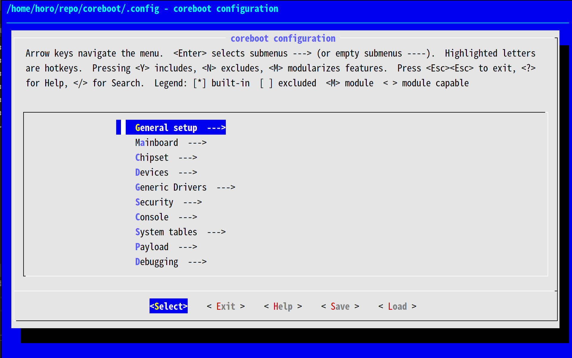
是不是和编译内核时很像? 😂 然后在 General Setup 里选中 Allow use of binary-only repoistory:
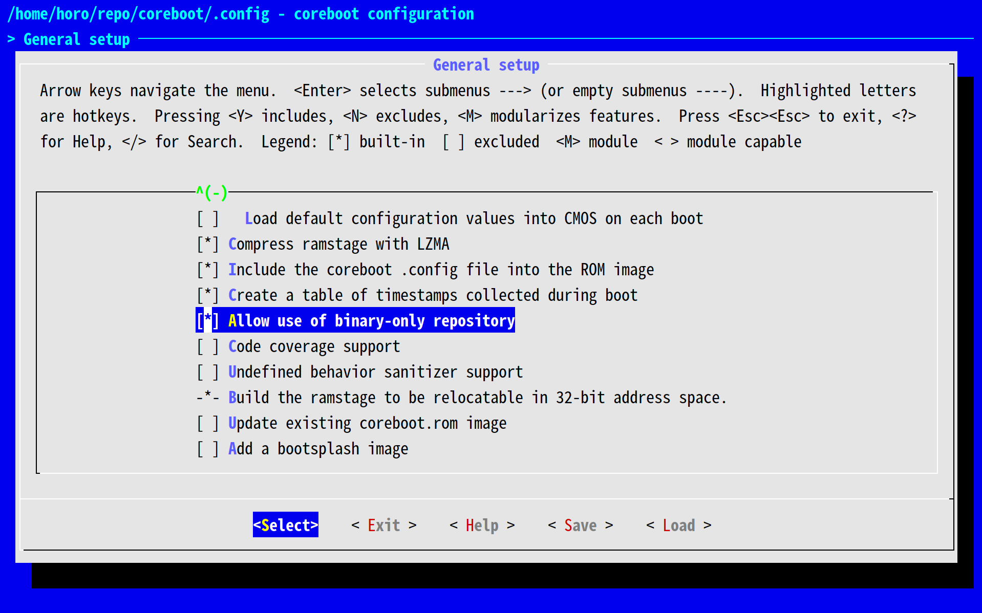
然后在 Board 一节里选择 Lenovo X230:
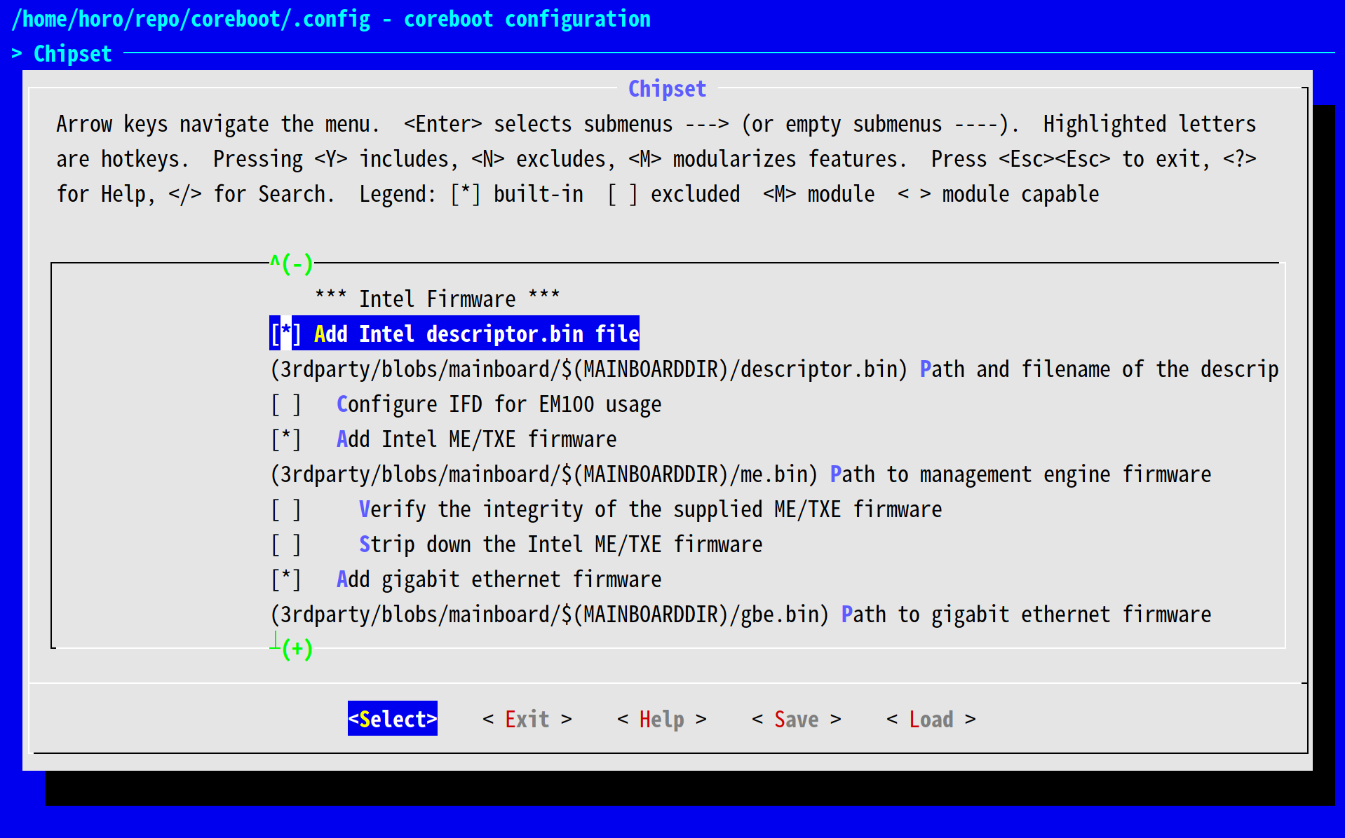
在 Chipset 中选择 Add Intel descriptor.bin file, Add Intel ME/TXE firmware 和 Add gigabit ethernet firmware,如果汝不是按刚才咱那样复制的话,记得改一下每一项 下面的文件位置选项:
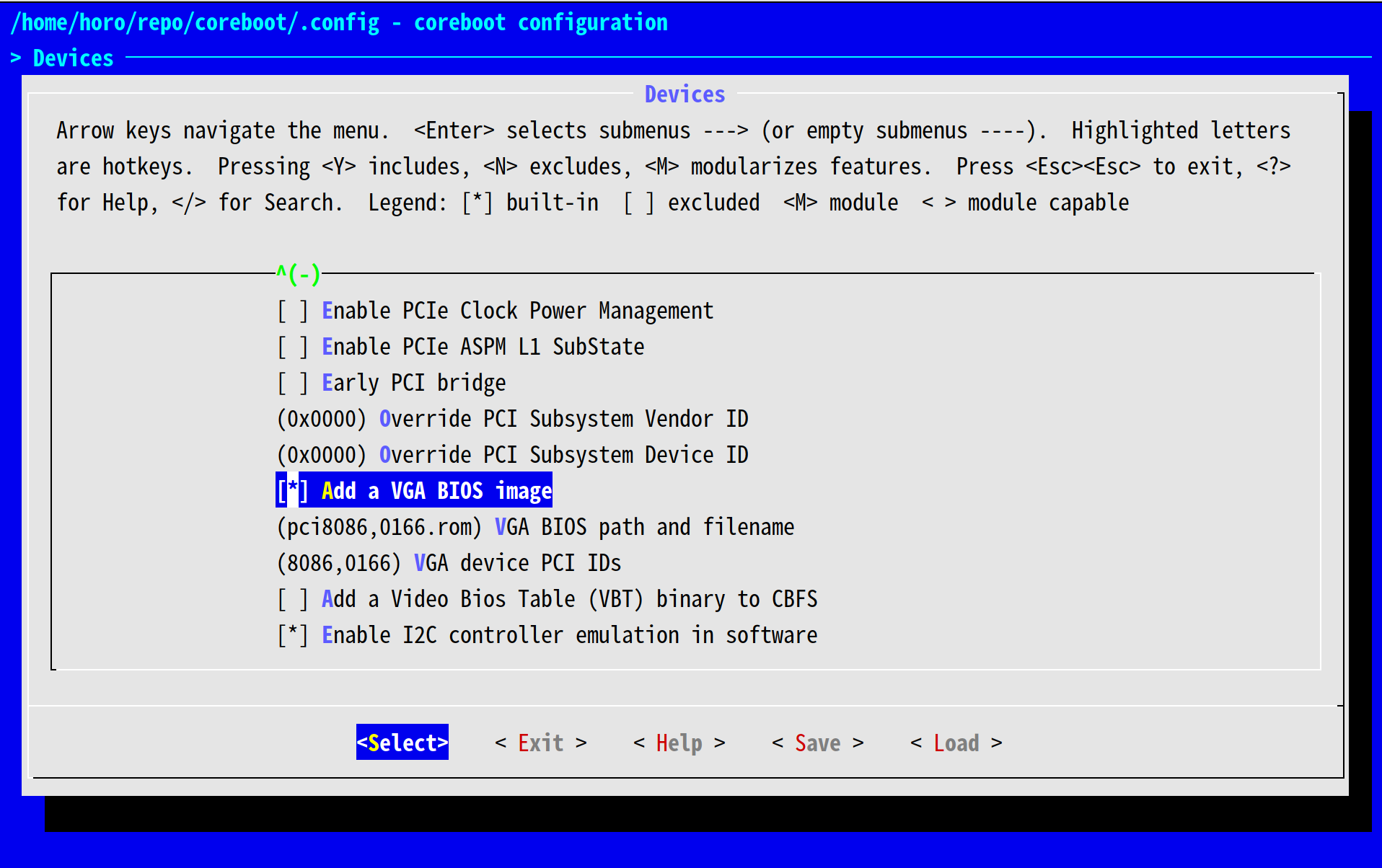
在 Display 一节中选择 Add a VGA BIOS image,如果汝不是按刚才咱那样复制的话, 记得改一下每一项下面的文件位置选项:
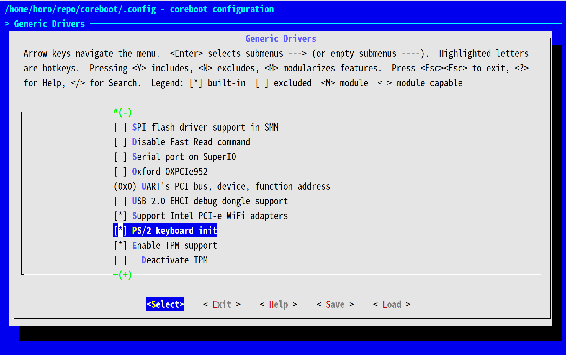
在 Generic Drivers 一节里选中 PS/2 keyboard init (有需要的话可以顺便启用一下 TPM 支持):
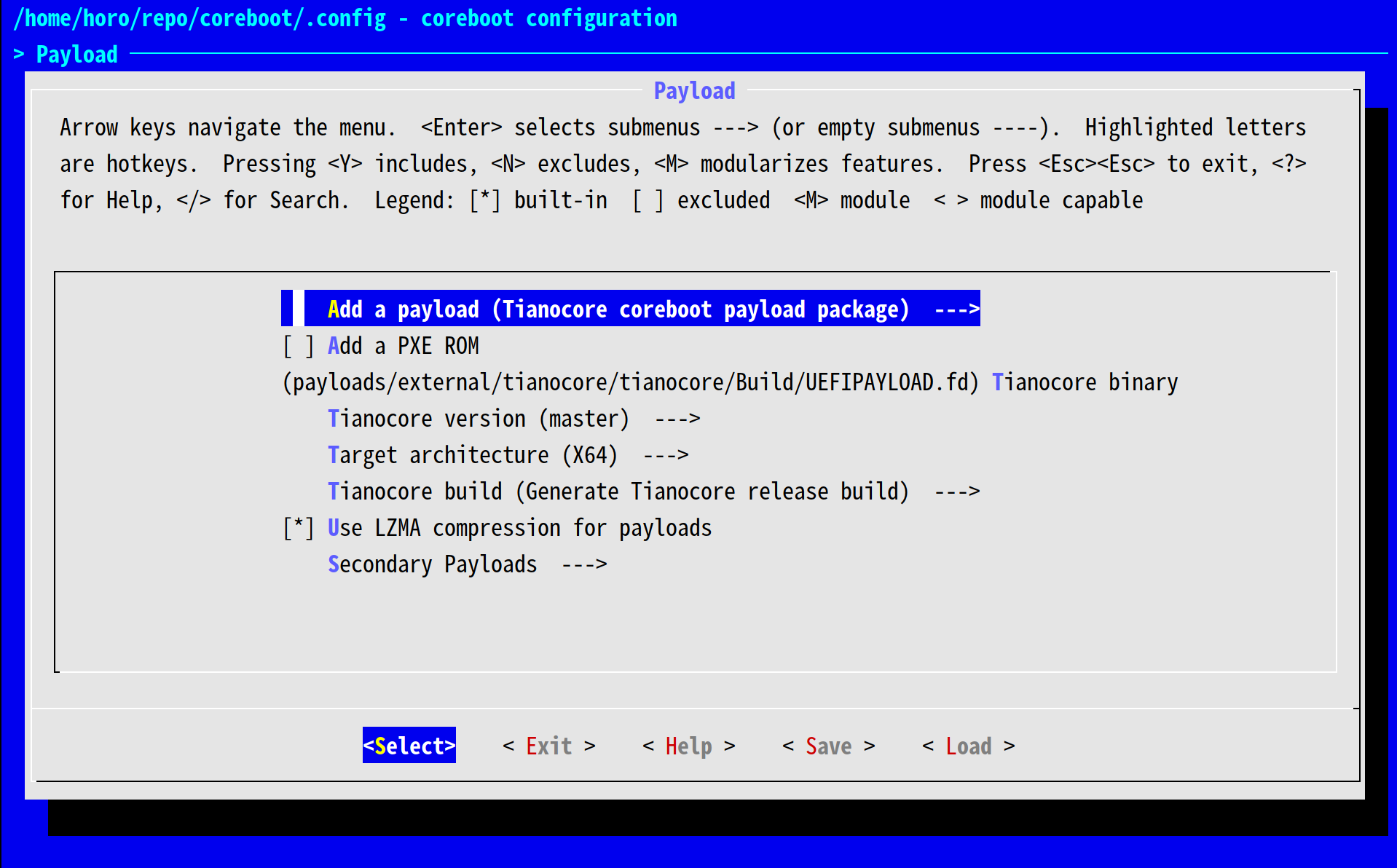
在 Payload 一节选择一个合适的 Payload (大概是启动管理器)?
- 默认的 SeaBIOS 是一个自由的 BIOS 引导实现。
- 也可以让 coreboot 引导 GRUB2 或者直接启动 Linux 内核(使用 grub 或者 linux payload, 前提是 BIOS 芯片里还有地方……)
- Tianocore 是一个开放源代码的 UEFI 实现。
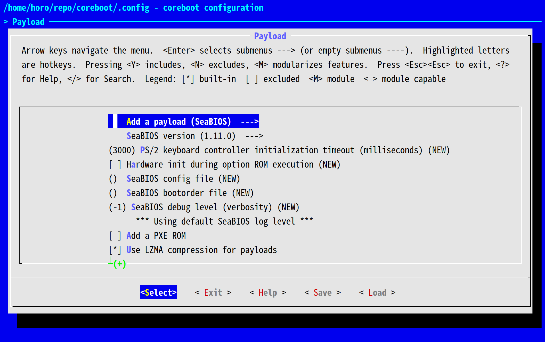
于是咱就用了 Tianocore ……
最后保存配置文件:
然后运行 make 编译汝的 ROM 吧(最后会在 build/coreboot.rom 里)。
刷入……
首先把 ROM 拆开成两个芯片大小,用 dd 就可以搞定:
dd of=top.rom bs=1M if=coreboot.rom skip=8
dd of=bottom.rom bs=1M if=coreboot.rom count=8
然后再接上编程器,首先刷入上面的芯片,看看可不可以正常开机 😂
flashrom -p linux_spi:dev=/dev/spidev0.0 -w top.rom -c MX25L3206E/MX25L3208E
如果可以的话,再刷入下面一块:
flashrom -p linux_spi:dev=/dev/spidev0.0 -w bottom.rom -c MX25L6406E/MX25L6408E
如果可以正常启动的话,Cheers!汝已经成功装上 coreboot 啦(白名单和 ME 的大部分功能也没啦……)
😂